


Locals protect space tech
 Print
Print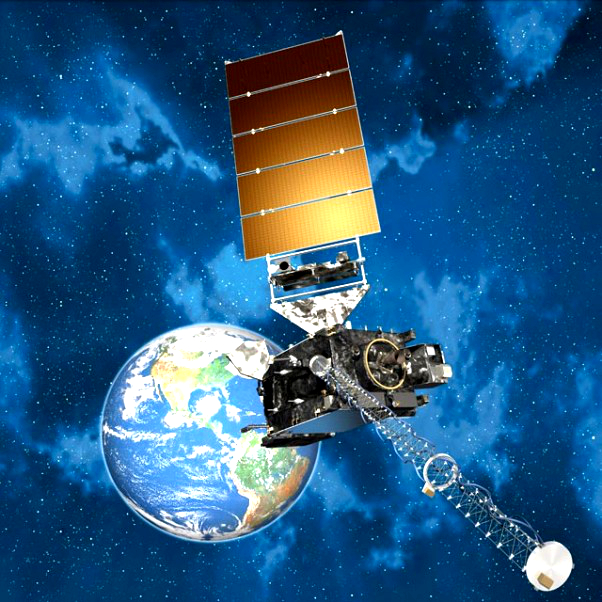 Australian researchers have helped develop advanced microelectronics that are resistant to harsh radiation in space.
A team of Melbourne researchers and international partners from the Italian Instituto Nazionale de Fisica Nucleare (INFN) and CERN, are developing radiation-hardened semiconductor chips.
Tests of the devices have relied on the unique state-of-art high energy ion microprobe on the SIRIUS ion accelerator at ANSTO’s Centre for Accelerator Science.
The studies were performed on a prototype SRAM chip built on nanoscale CMOS technology for use in space, and high energy accelerator or nuclear facilities where operating control systems are exposed to radiation.
The prototype SRAM memory chip features a new architecture using an original approach to eliminate single event upsets (SEUs) and single event effects (SEEs) to boost its operating reliability in radiation hard environments.
The SIRIUS microprobe system can generate and focus a large variety of ion beams and allows a user to select a linear energy deposition rate in a preselected region of the chip at a penetration depth.
Radiation can produce parasitic signals or damage crucial electronic components of operating control systems, such as memory and processing chips, which are used in space satellites, instruments and vehicles.
“The impact of radiation damage to the performance of the newest generations of microelectronic technologies is still not very well understood in the scientific community,” says scientist Dr Jafar Shojaii.
“Only an experiment can confirm that the performance of the technology will not be adversely impacted by radiation..
“We need to validate that the hundreds of millions of transistors in a single chip will perform suitably at the device level, before use in space. The radiation effects on semiconductor chips have been one of the main reasons for satellite failures in space missions.
“Our program is greatly supported by the Department of Defence, as this novel capability is extremely important in defence applications.”
The custom chip was tested under different laboratory conditions, such as different particle mass and energy, increasing particle rate and increasing accumulated dose, over the course of three experiments performed at ANSTO in the last 12 months.
An absorbed radiation dose by an electronic component is usually expressed in Rads. The new chip architecture proved to be radiation hard for threshold doses required by a space community (100s of kRads) and particle rates up to 10 MHz.
Moreover, the chip was able to withstand very high doses up to 100 MRad range, which is required by the high energy accelerator community, such as the Large Hadron Collider experiment at CERN in Switzerland.